SEIML HW1: Getting started with the AMD-Xilinx development environment⚓
Objective of the lab⚓
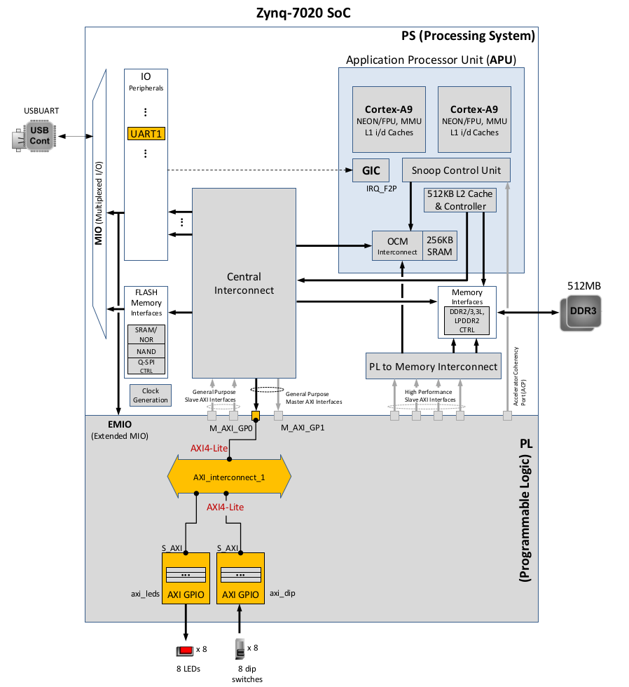
The objective of this first lab is to take in hand the embedded systems development environment proposed by AMD-Xilinx and to illustrate the course on embedded processors through a simple system integrating the ARM Cortex-A9 processor and targeting the ZedBoard. You will use Vivado to create the system and Vitis (Unified Software Platform) to create a simple application to check the functionality of the system.
Part 1. Create a Vivado project for a Zynq system⚓
In the first part of this lab, you will create a Vivado project for the Processing System (PS) alone, i.e. for Zynq Cortex A9, without using the Programmable Logic (PL) part of the Zynq. This includes the following tasks:
- Create a Vivado project for a Zynq system
- Use the IP Integrator to create a hardware system
- Use Vitis (Unified Software Platform) to create a standard memory test project
- Run the test application on the board and hence verify hardware functionality
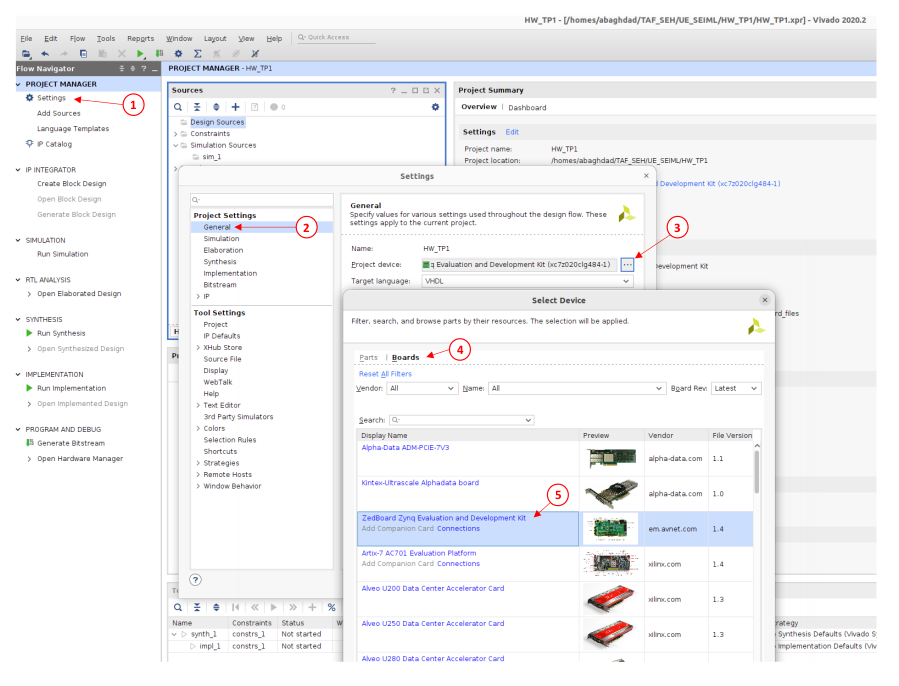
A. Create a Vivado Project⚓
- Open a terminal and setup the Vivado-Vitis environment through the command:
1SETUP MEE_VITIS20202 - Open Vivado:
1vivado & - Click Create Project to start the wizard. You will see the Create a New Vivado Project dialog box. Click Next.
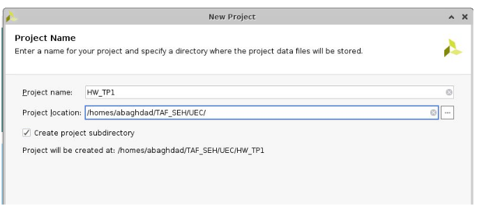
- Click the Browse button of the Project Location field of the New Project and browse to an appropriate directory of your network disk {e.g.
/homes/”your_login”/TAF_SEH/UE_SEIML/}, and click Select. - Enter HW_TP1 in the Project Name field. Make sure that the Create Project Subdirectory box is checked. Click Next.
- In the Project Type form select RTL Project, and click Next
- In the Add Sources form, select VHDL as the Target language and Mixed as the Simulator language, and click Next
- Click Next one more time to skip Adding Constraints
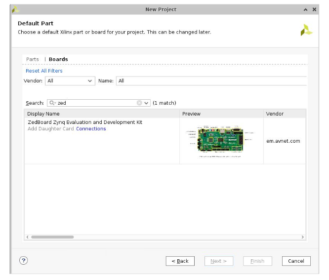
- In the Default Part window, select the Boards tab, search for the ZedBoard, select it and click Next.
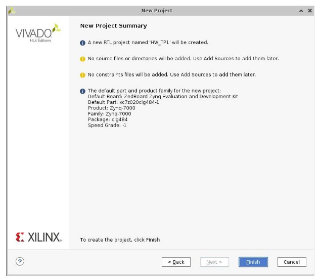
- Check the Project Summary (should be similar to what you see below) and click Finish to create an empty Vivado project.
In case there is an issue in selecting the ZedBoard (Bug in some tool versions), you need to check and change the settings from inside Vivado once the project is opened as indicated in the screen copy below.
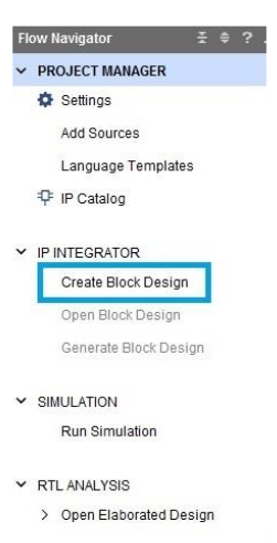
B. Creating the System Using the IP Integrator⚓
- In the Flow Navigator, click Create Block Design under IP Integrator
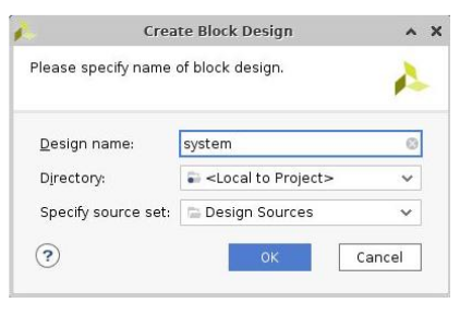
- Enter system for the design name and click OK
- Right-click anywhere in the Diagram workspace and select Add IP.
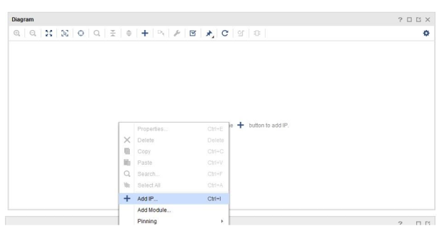
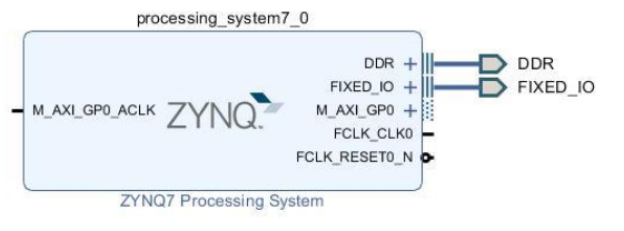
- Once the IP Catalog opens, type “zyn” into the Search bar, find and double click on ZYNQ7 Processing System entry, or click on the entry and hit the Enter key to add it to the design.
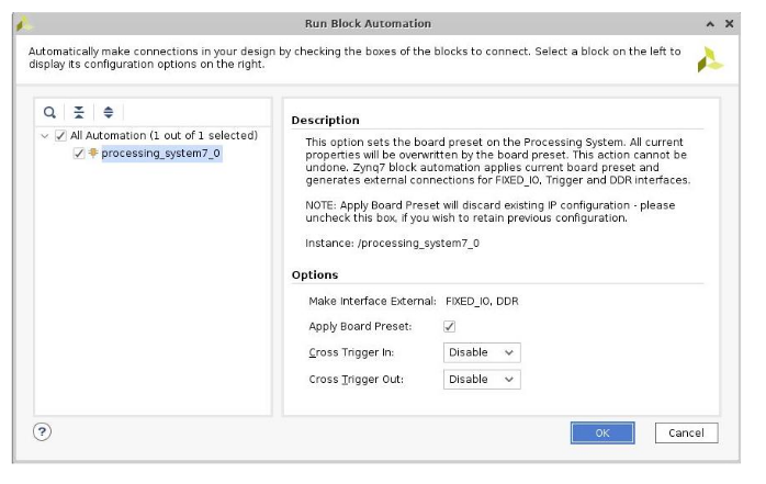
- Notice the message at the top of the Diagram window in a green label saying that Designer Assistance available. Click Run Block Automation.
- A new window pops up called the Run Block Automation window. In it, select /processing_system7_0, leave the default settings and click OK
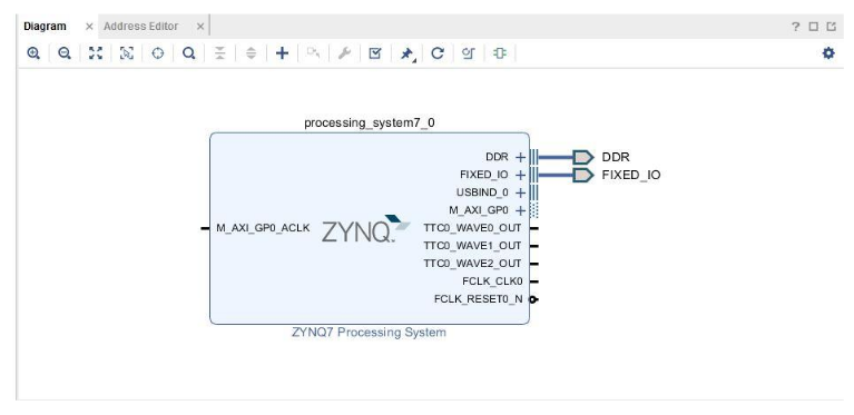
- Once Block Automation has been complete, notice that ports have been automatically added for the DDR and Fixed IO, and some additional ports are now visible. The imported configuration for the Zynq related to the board has been applied which will now be modified. The block should finally look like this:
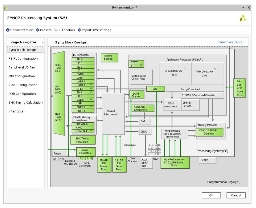
- Double-click on the added block to open its Customization window. Notice now the Customization window shows selected peripherals (with tick marks). This is the default configuration for the board applied by the block automation.
C. Configure the processing block with just UART 1 peripheral enabled⚓
- A block diagram of the Zynq should now be open, showing various configurable blocks of the Processing System.
- At this stage, the designer can click on various configurable blocks (highlighted in green) and change the system configuration.
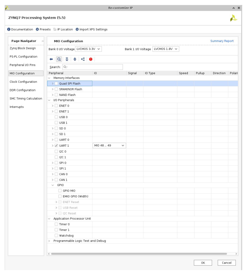
- Click on one of the peripherals (in green) in the I/O Peripherals block of the Zynq Block Design, or select the MIO Configuration tab on the left to open the configuration form
- Expand I/O peripherals if necessary, and ensure all the following I/O peripherals are deselected except UART 1.
i.e. Remove:- ENET
- USB 0
- SD 0
- Expand GPIO to deselect GPIO MIO
- Expand Memory Interfaces to deselect Quad SPI Flash
- Expand Application Processor Unit to disable Timer 0.
- Select the PS-PL Configuration tab on the left.
- Expand AXI Non Secure Enablement > GP Master AXI interface and deselect M AXI GP0 interface.
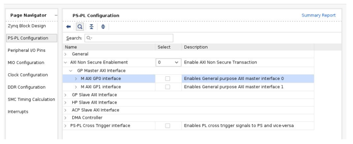
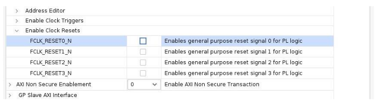
- Expand General > Enable Clock Resets and deselect the FCLK_RESET0_N option.
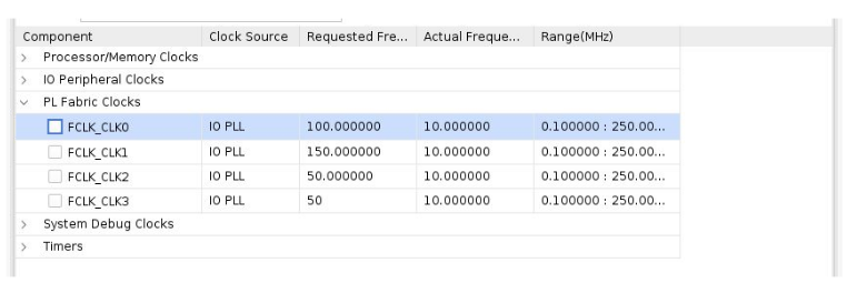
- Select the Clock Configuration tab on the left. Expand the PL Fabric Clocks and deselect the FCLK_CLK0 option and click OK.
- Click on the Regenerate Layout button (green arrow) shown below:
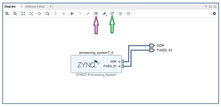
- Click on the Validate Design button (purple arrow) and make sure that there are no errors!
D. Generate Top-Level and Export to Vitis⚓
-
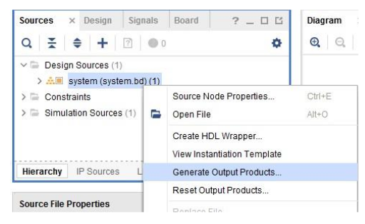
In the sources panel, right-click on system.bd (system Block Diagram), and select Generate Output Products… and click Generate to generate the Implementation, Simulation and Synthesis files for the design (You can also click on Generate Block Design in the Flow Navigator pane to do the same)
-
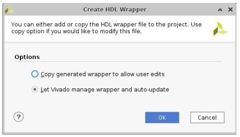
Right-click again on system.bd, and select Create HDL Wrapper… to generate the top-level VHDL model. Leave the Let Vivado manage wrapper and auto-update option selected, and click OK
The system_wrapper.vhd file will be created and added to the project. Double-click on the file to see the content in the Auxiliary pane.
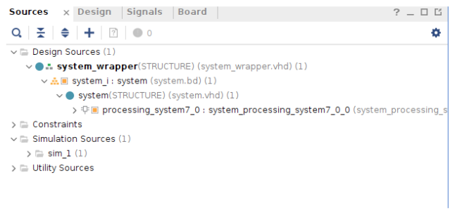
- Notice that the VHDL file is already Set As the Top module in the design, indicated by the icon. In fact, the wrapper defines the Block Design as the top-level design, so you can synthesize, implement, and generate a bitstream for the block design.
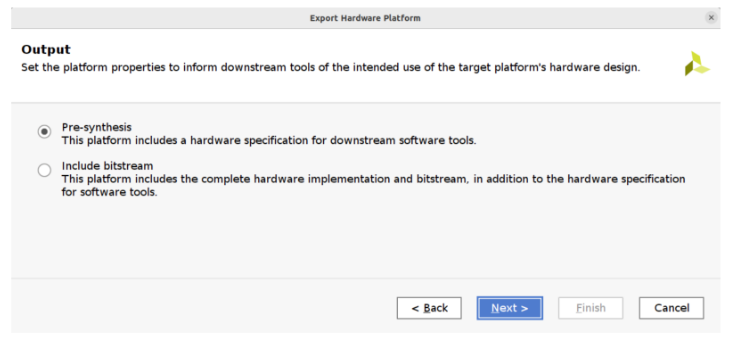
- Select File > Export > Export hardware and click OK. (Save the project if prompted) Note: Since in this first simple project we do not have any hardware in Programmable Logic (PL) there is no bitstream to generate, hence the Include bitstream option is not necessary at this time.
Therefore, in the Output screen, you can select to export only the hardware specification (Pre-synthesis). click Next to continue.
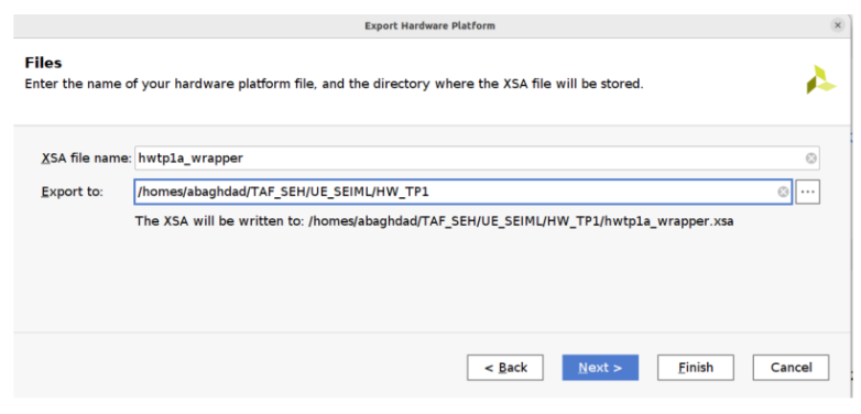
The Files screen gives you the option to choose a name for the Xilinx Shell Architecture (XSA) file, and provide a path to a folder that the file will be placed within. Give your XSA file a name (e.g. hwtp1a_wrapper). For the location, you can keep the default one inside your HW_TP1 folder. This file will later be imported into Vitis (for the software development), so take a note of where it is placed and what it is called.
Important: Do not use spaces in the file name or export path. Underscores or camelCase are recommended instead.
Click Next to continue.
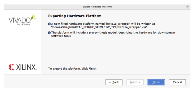
The final screen of the wizard summarizes the options you selected. Click Finish.
- Launch Vitis for software development: Vitis can be launched directly from a terminal through the command
vitis &or from Vivado by selecting Tools > Launch Vitis IDE.
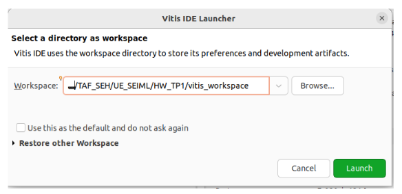
Upon launching Vitis, a dialog will appear where a workspace must be chosen. The workspace is the directory where all of the projects and files for the application being developed will live. If a folder that does not currently exist is chosen, it will be created. Choose a workspace inside your HW_TP1 directory and click Launch to finish launching Vitis.
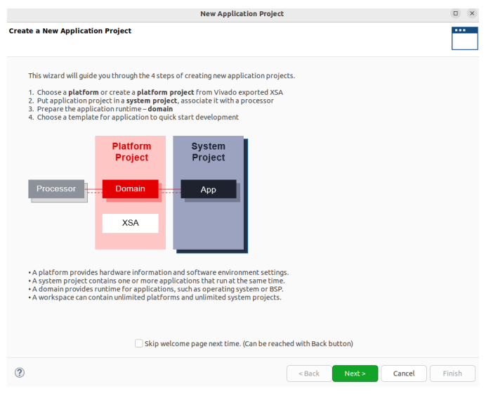
E. Generate Memory TestApp in Vitis⚓
With Vitis open, an application project must be created to hold your source files. In creating an application project, a hardware platform will also be created from an XSA file previously exported from Vivado.
-
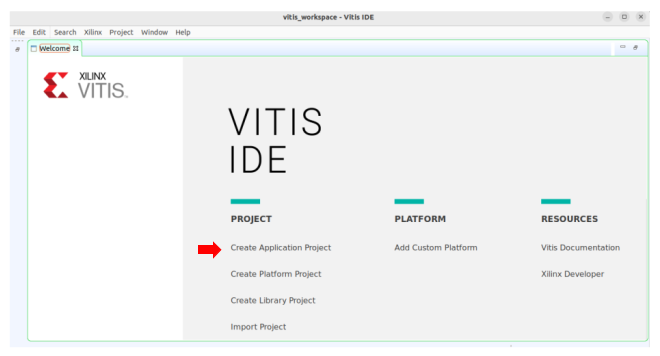
On Vitis' welcome screen, click Create Application Project. The wizard that launches will be used to create and configure a new application.
-
The first screen of the wizard is a welcome page, which summarizes what each of the components of a software design are. Click Next to continue.
-
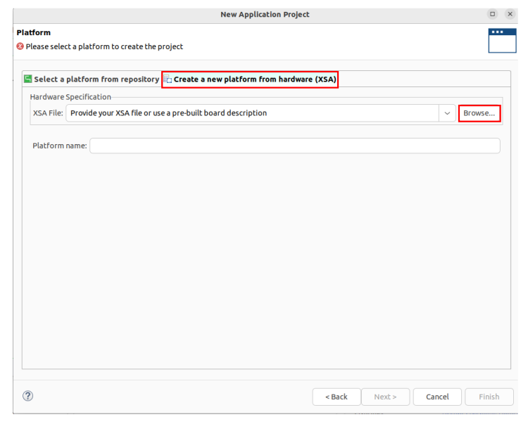
Next, the platform that the application targets must be created. Open the Create a new platform from hardware (XSA) tab.
-
Browse your file system to find the Xilinx Shell Architecture previously exported from Vivado. With the XSA file highlighted, click Open to select it and return to the Platform screen of the wizard.
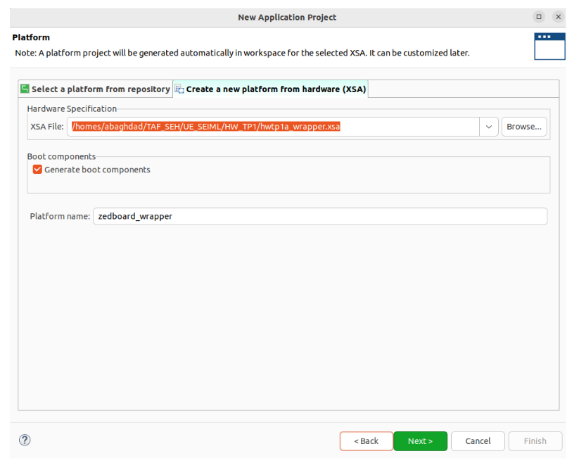
Once you have found the XSA file and opened it, make sure that it is selected in the Hardware Specification list.
Give your platform a name (e.g. zedboard_wrapper).
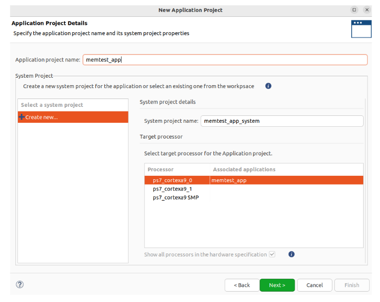
The Generate boot components box can be used to automatically build all of the additional components necessary to boot the application from flash memory or an SD card. Leaving this box checked is recommended. Click Next to continue. - The next screen is used to set some options for the application project and the system project. The names of both projects need to be set, as well as which processor core will be used to run the application. You can choose memtest_app as application project name. All settings can be left as defaults. Click Next to continue.
Note: A system project can contain multiple application projects, which can all be run at once.
- Next, the domain that the application project operates in will be defined. In this case all default settings will be used. Click Next to continue.
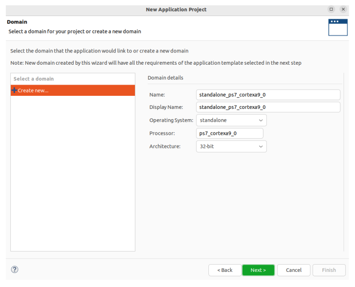
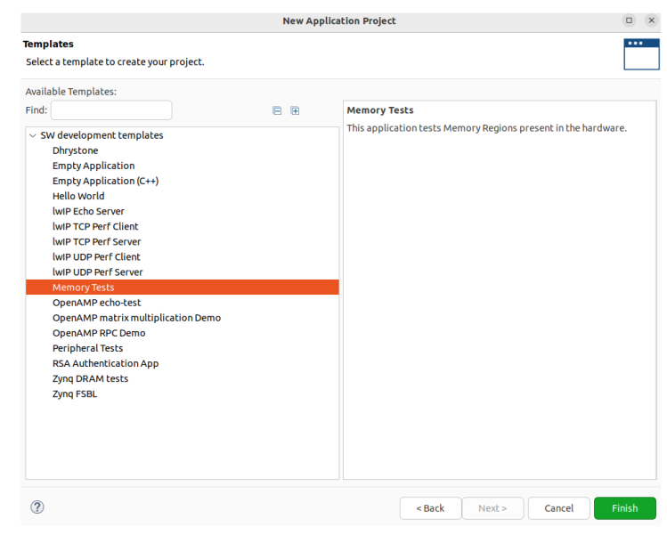
- Lastly, a template project will be chosen. Each template pre-configures the application project for a different purpose. For this first project, select Memory Tests from the list of Available Templates. Click Finish to finish creating the project.
The memtest_app project will be created and will be visible in the project Explorer pane of Vitis. - Expand the folders in the project Explorer pane on the left, and observe the different generated files. The zedboard_wrapper is the platform that the application targets, which provides hardware information and software environment settings. The memtest_app_system is the system project that contains one or more application that run at the same time. In our case, only one application exists which is memtest_app. Inside the application, open the memorytest.c file under src folder, and examine its content. This file calls the functions to test the memory.
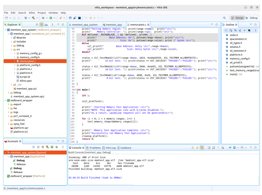
- Build the Vitis Application: Once an application project has been set up and includes all necessary sources, it should be built. To build the project and all of its dependencies, select the [System] project in the Assistant pane, and either click the Build button ( ) or press Ctrl-B on your keyboard.
Note: There are three types of build targets in the Assistant pane, Platforms, Systems, and Applications. Building the application will not trigger any other applications in the system to be built, but will build the wrapper as a dependency. Building the platform will only build the platform, as it has no dependencies. Building the system causes each application in the system, as well as the platform, to be built.
This process may take some time to complete. When done, the Console tab at the bottom of the window will display a “Build Finished” message.
F. Test in Hardware⚓
- Ensure that the ZedBoard is connected to the machine and powered-on. Two micro-usb cables should be used between the host machine and the PROG and the UART connectors of the board. The board should be placed in the JTAG mode.
- In order to verify the operation of the hardware (ARM Cortex A9) by using the memtest application, you should now execute it on the processor, and observe the output in a serial terminal window.
In order to prepare a serial terminal window in the host machine, open a terminal and execute the following command line:This will connect a serial terminal to the appropriate COM port and configure it with the appropriate parameters (related to that of the ZedBoard UART1! i.e. Baud Rate of 115200, 8 data bits, 1 stop bit, no parity and no flow control).1env GDK_BACKEND=x11 putty -serial /dev/ttyACM0 -sercfg 115200,8,n,1,N
Il you wish, you can create an alias for this command that you can use in the rest of SEIML labs. In your home directory, if you have a file with the name .profile.PERSO you can add in it the following line (otherwise, you can create a file with this name and add the line in it):With that done, the alias “puttyz” will be active automatically when you lunch a new terminal.1alias puttyz='env GDK_BACKEND=x11 putty -serial /dev/ttyACM0 -sercfg 115200,8,n,1,N'
Note: While Vitis has a built in serial terminal included in its Debug view, it sends characters to a board on a line-by-line basis. Some software examples require the use of character-by-character reception of data. PuTTY (or Tera Term) is recommended if you are not sure what will work. - Run the memtest application and verify the functionality as follows:
In the Explorer pane at the left side of the screen, right click on the application project that is to be run, and select Run as > 1 Launch on Hardware (Single Application Debug). The FPGA will be programmed with the bitstream (no bitstream in this first project example, only the ARM Cortex A9 is used!), the ELF file created by the software build is loaded into system memory, and the application project will begin to run.
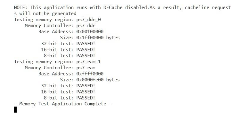
Note: Once the project has been run at least once, you can use the green run button in the toolbar at the top of the screen to program the board instead. - You should see the following output on the serial terminal window (putty).
- Close Vitis by selecting File > Exit.
Part 2. Adding IP cores in the Programmable Logic (PL)⚓
In this second part of the lab, you will add two IP cores in the Programmable Logic (PL) of the Zynq to implement the complete embedded system shown in the first page of this lab.
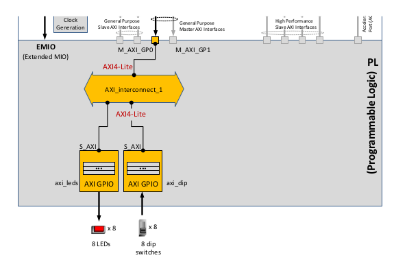
A. Add Two Instances of GPIO⚓
- Go back to Vivado. In the Sources panel, expand system_wrapper, and double-click on the system.bd (system_i) file to invoke IP Integrator.
- Double click on the Zynq block in the diagram to open the Zynq configuration window.
- Select PS-PL Configuration page menu on the left.
We should now (re)activate the interface between PS and PL. - Expand AXI Non Secure Enablement > GP Master AXI Interfaces and click on Enable M_AXI_GP0 interface check box to enable the AXI GP0 port.
- Expand General > Enable Clock Resets and select the FCLK_RESET0_N option.
- Select the Clock Configuration tab on the left. Expand the PL Fabric Clocks and select the FCLK_CLK0 option (with requested clock frequency of 100 MHz) and click OK.
- Notice the additional M_AXI_GPO interface, and M_AXI_GPO_ACLK, FCLK_CLK0, and FCLK_RESET0_N ports are now included on the Zynq block. You can click the regenerate button to redraw the diagram to get something like this:
- Next, in the block Diagram pane's toolbar, click the Add IP button ( ) and search for AXI GPIO in the catalog.
- Double-click the AXI GPIO to add the core to the design. The core will be added to the design and the block diagram will be updated.
- Click on the AXI GPIO block to select it and, in the Block Properties tab on the left, change the name to switches.
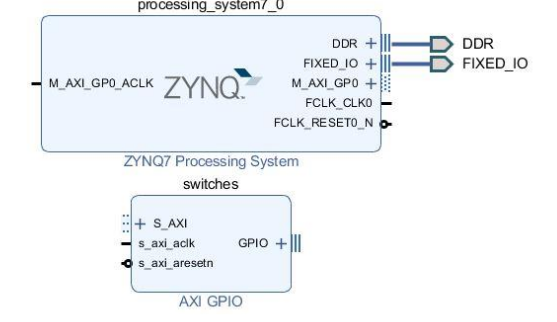
- Double click on the AXI GPIO block to open the customization window.
- From the Board interface drop down, select sws 8bits for GPIO IP Interface (this was predefined as we started the creation of the project by targeting the ZedBoard, therefore its definition and available peripherals are included in Vivado).
- Next, click the IP configuration tab, and notice the width has already been set to match the switches on the Zedboard (8).
- Click OK to save and close the customization window
- Notice that Designer assistance is available. Click on Run Connection Automation, and select /switches/S_AXI
- Click OK when prompted to automatically connect the master and slave interfaces. The blocks can be dragged to be rearranged, or the design can be redrawn. You can click the regenerate button to redraw the diagram to get something like this:
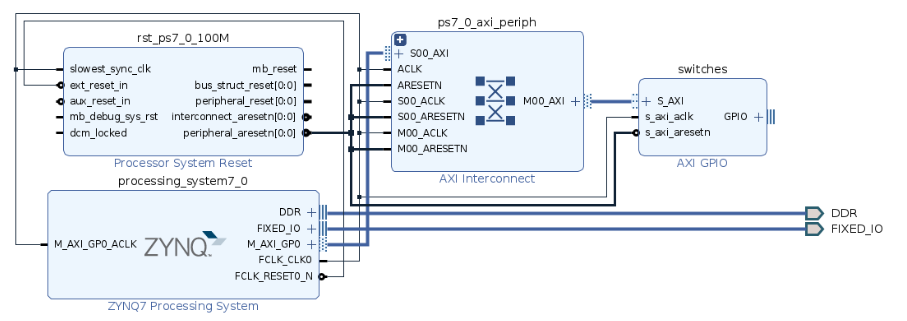
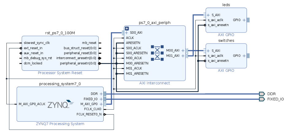
Notice that two additional blocks have automatically been added to the design: Processor System Reset and AXI Interconnect. - Add another instance of the GPIO peripheral (Add IP). Name it as leds
- Double click on the IP block, select “leds 8bits” for GPIO IP Interface and click OK. At this point, connection automation could be run, or the block could be connected manually. This time the block will be connected manually.
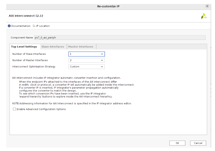
- Double click on the AXI Interconnect (name : ps7_0_axi_periph) and change the Number of Master Interfaces to 2 and click OK
- Click on the S_AXI port of the leds AXI GPIO block (name: leds), and drag the pointer towards the AXI Interconnect block. The message ‘Found 1 interface’ should appear, and a green tick should appear beside the M01_AXI port on the AXI Interconnect indicating this is a valid port to connect to. Drag the pointer to this port and release the mouse button to make the connection.
- In a similar way, connect the following ports:
- leds s_axi_aclk -> Zynq7 Processing System FCLK_CLK0
- leds s_axi_aresetn -> Processor System Reset peripheral_aresetn
- AXI Interconnect M01_ACLK -> Zynq7 Processing System FCLK_CLK0
- AXI Interconnect M01_ARESETN -> Processor System Reset peripheral_aresetn
The block diagram should look similar to this:
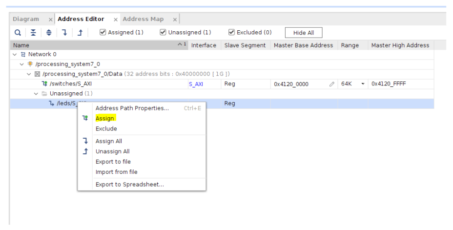
- Click on the Address Editor tab, and if necessary expand processing_system7_0 / Data / Unassigned
- Notice that the switches instance has been automatically assigned an address, but leds has not (since it was manually connected). Right click on leds and select Assign.
B. Make GPIO Peripheral Connections External⚓
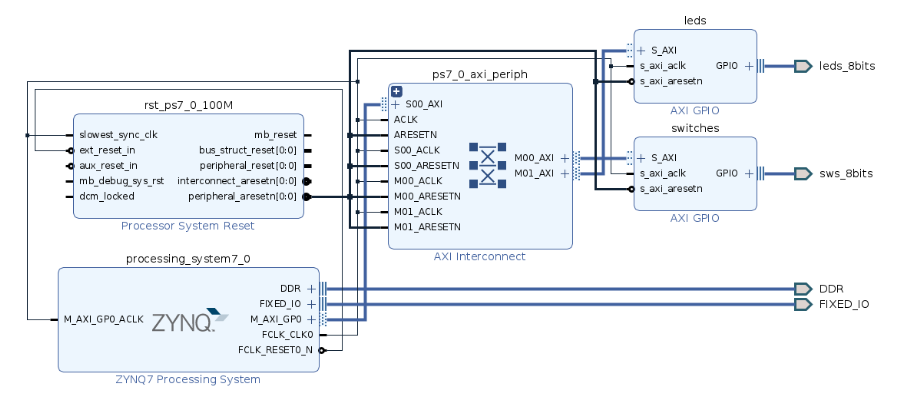
- In the Diagram view, notice that Designer Assistance is available. However, we will manually create the ports and connect them.
- Right-Click on the GPIO port of the switches instance and select Make External to create the external port. This will create the external port named GPIO_0 and connect it to the peripheral. As we have selected the ZedBoard as target, which is known by Vivado, the pin constraints will be automatically applied to the port!
- Select the GPIO_0 external port and change the name to sws_8bits in its properties form. The width of the interface will be automatically determined by the upstream block.
- For the leds GPIO, select it and click on the Run Connection Automation link.
- In the opened GUI, select leds_8bits under the Options section. Click OK.
- Run Design Validation (either by a click on in the toolbar or through Tools > Validate Design) and verify there are no errors. The design should now look similar to the diagram below
- In the Flow Navigator, click Run Synthesis. (Click Save if prompted) and when synthesis completes, select Open Synthesized Design and click OK
- In the shortcut Bar on the upper-right, select I/O Planning view from the Layout dropdown menu
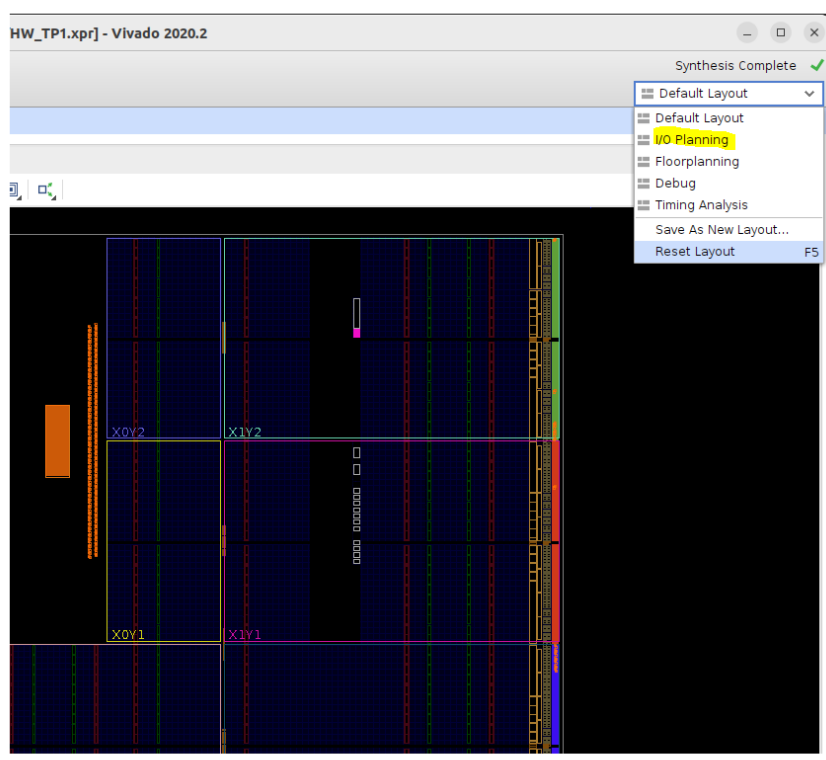
- In the I/O Ports tab, expand the two external GPIO ports, and expand leds_8bits_tri_o, and sws_8bits_tri_i, and notice that the ports have been automatically assigned pin locations, along with the other Fixed IO ports in the design, and an I/O Std of LVCMOS33 and LVCMOS25 have been applied. If they were not automatically applied, pin constraints can be included in a constraints file, or entered manually or modified through the I/O Ports tab.
C. Generate Bitstream and Export to Vitis⚓
- Click on Generate Bitstream, and click Yes if prompted to Launch Implementation (Click Yes if prompted to save the design)
- Click Cancel to the pop up that appears at the end notifying the Bitstream generation successfully completed.
- Now, as you have done in the first part of this lab, export the hardware by clicking File > Export > Export Hardware and selecting “Include bitstream”. This time, there is hardware in Programmable Logic (PL) and a bitstream has been generated and should be included in the export to Vitis.
Give your XSA file a name (e.g.hwtp1b_wrapper). For the location, you can keep the default one inside your HW_TP1 folder. This file will later be imported into Vitis (for the software development). - Click Next and then Click Finish to export the hardware platform.
- Launch Vitis as you have done previously with the same workspace.
D. Generate Software Application in Vitis⚓
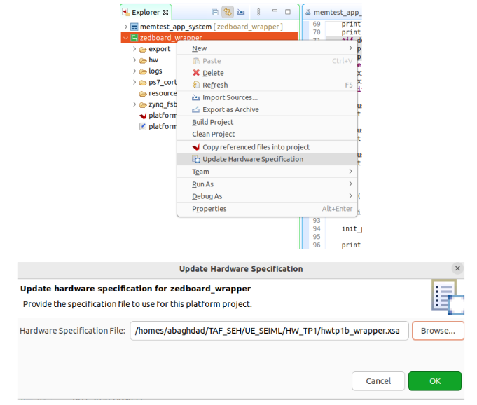
- In Vitis, you need first to update the hardware platform by selecting the existing one “zedboard_wrapper” in Explorer pane, right-clicking and selecting “Update Hardware Specification” from the menu. You will then be required to browse to the newly exported file hwtp1b_wrapper.xsa, followed by two OKs.
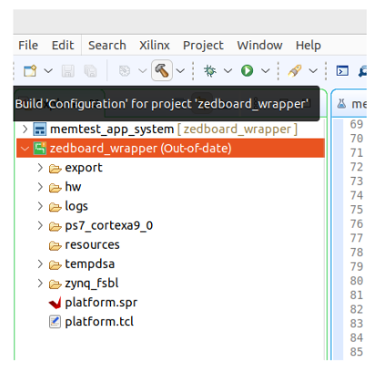
The new platform project can then be built through right-clicking as shown below:
- From the File menu select File > New > Application Project
- In the opened wizard, click Next, then for the Platform choice select the existing platform “zedboard_wrapper” and click Next.
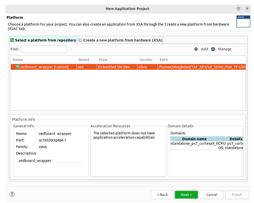
- Specify the application project name (e.g.
hwtp1b_app) and keep all other options in defaults values, which implies the creation of a new System project namelyhwtp1b_app_system. Note that in standalone (no operating system), each System project can comprise only one application. - Next, the domain that the application project operates in will be defined. In this case default settings will be used, which means selecting the already defined “standalone” runtime. Click Next to continue.
- Select Empty Application from the list of templates and click Finish. This will create a new Application and System projects using the updated Platform project.
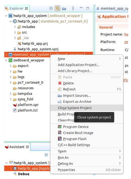
- In order to simplify the Explorer and Assistant views, you can close the memtest_app_system project from the Explorer pane by a right-click on it and selecting “Close System Project”.
- Expand hwtp1b_app in the Explorer pane, and right-click on the src folder, and select Import Sources.
- An application source code is provided in Moodle (
hw_tp1.c), download it, and browse to the download folder to select it. - Select
hw_tp1.c and click Finish - Spend some time analyzing and understanding the structure and functionality of the given simple application code. Examine the Xilinx functions for GPIO which are declared in xgpio.h header file. Also have a look at the contents of the xparameters.h file. The xparameters.h file contains the address map for the peripherals of the system. This file is generated from the hardware platform description from Vivado. It includes in addition several #define used to identify each of the peripherals.
- Two lines of code are left to be completed by you in the provided simple software application code (hw_tp1.c) with associated comments. Spend some time to find the appropriate functions and parameters to be used.
- Build the new Vitis application as you have done for memtest_app (select the [System] project in the Assistant pane and click the Build button). The executable "hwtp1b_app.elf" will be generated if there are no errors! If there are errors, correct them by referring to the xparameters.h file.
E. Test in Hardware⚓
We will use the same flow as in the first part of this lab (however this time a bitstream of the generated hardware will be downloaded to the PL part of the Zynq).
- As in the first part of this lab, in the Explorer pane at the left side of the screen, right click on the application project that is to be run, and select Run as > 1 Launch on Hardware (Single Application Debug). The FPGA will be programmed with the bitstream, the ELF file (hwtp1b_app.elf) created by the software build is loaded into system memory, and the application project will begin to run.
- You should see something similar to the following output on UART Terminal console
- Why the display of the messages on the UART Terminal is slow? What is the speed of display and how it is implemented? What is the impact of such kind of delay implementation?
- How could we exit the application that runs in a loop?!
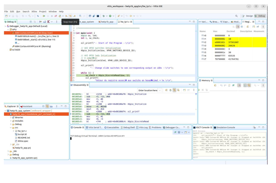
- Restart the software application, this time with the Debug As > Launch on Hardware command. Run line by line, add breakpoints, explore the various possibilities offered by this debugging interface (e.g. viewing registers, assembler code, etc.).
Identify the assembler instruction that corresponds to reading the value of the switches?
Execute line by line and check the value of the register defined in the instruction. Note the various sub-functions called (you need to use Step Into (next to Step Over) the right functions).

- Close Vitis and Vivado programs by selecting File > Exit in each program
- Power OFF the board!
To be continued... !