SEIML HW2: Peripherals and Interrupts⚓
Objective of the lab⚓
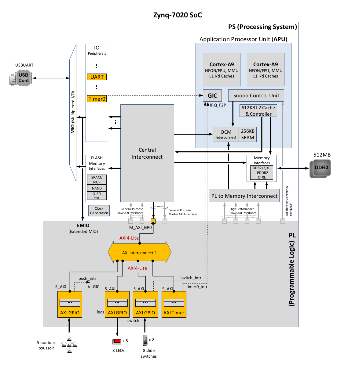
The objective of this lab is to illustrate the integration of standard peripherals and the implementation of interruptions in an embedded system. The aim is to extend the system developed in the previous lab to implement the system illustrated in Figure 1 below.
A. Design and configuration of the hardware architecture, including interrupts⚓
- Open a terminal and setup the Vivado-Vitis environment through the command:
1SETUP MEE_VITIS20202 - Open Vivado:
1vivado & - Open the project of the previous lab:
HW_TP1 - You will now create a copy of this project into
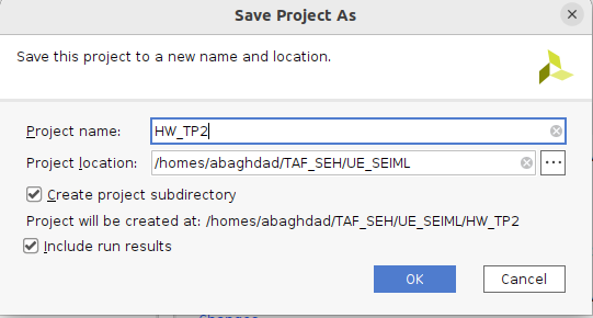
HW_TP2to continue from the work done during the previous lab session. You can do this by selectingFile > Project > Save As…and giving the nameHW_TP2as show below.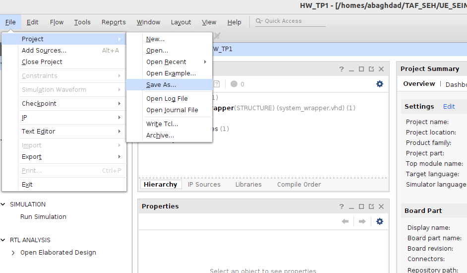
This will duplicate the project in a separated folder. - Open the block design of the project by expanding
system_wrapperinSourcespanel, and double-click on thesystem.bd(system_i) file to invoke IP Integrator. - Configuration of the Processing System (PS): double click on the Zynq block in the block diagram of the system to open the Zynq configuration window. Enable Timer 0 of the PS as shown in Figure 1 (
MIO Configuration tab > Application Processor Unit). This PS-Timer 0 will not be used in this lab, but will be needed later on, in the software labs using Linux. - Configuration of the Programmable Logic (PL):
- Follow the same approach that has been detailed in the previous lab to add the required peripherals (
AXI GPIOandAXI Timer) as show in Figure 1. - Rename and configure the added standards peripherals appropriately.
- Connect them to the rest of the system (refer to
HW_TP1for the flow) - Enable interrupts for the buttons and the switches. Interrupt of axi_timer is enabled by default.
- Connect these three interrupt sources to the Cortex-A9 processor unit through its input interrupt port IRQ_F2P. To do so, we need first to add a concat block. The concat block merges the three interrupt signals into a 3-bit vector. Note that you can still connect it to
IRQ_F2P[0:0]. When you run the synthesis, Vivado will update it toIRQ_F2P[0:2]- Add the concat block (Add IP menu, as for
AXI GPIOandTimer) - Select and double-click it to customize the number of input ports to 3.
- Connect the interrupt outputs of axi_timer, buttons, and switches to the inputs of the concat block.
- Connect the output of the concat block to
IRQ_F2P[]. For that, you need to enable interrupts in the Cortex-A9 Zynq PS as follows:
- Add the concat block (Add IP menu, as for
- You can click the regenerate button to redraw the diagram.
- Verify the memory map in Address Editor tab, i.e. all peripherals have been assigned address spaces and there are no unmapped blocks.
- Follow the same approach that has been detailed in the previous lab to add the required peripherals (
B. Make GPIO Peripheral Connections External⚓
- If you have not used Run Connection Automation designer assistance, you can use the same flow as in
HW_TP1to make external the GPIO port of the buttons peripheral as illustrated in Figure 1. - Select the created external port and change its name to
btns_5bits. - Run Design Validation (
Tools -> Validate Design) and verify there are no errors. The design should now look similar to the diagram below.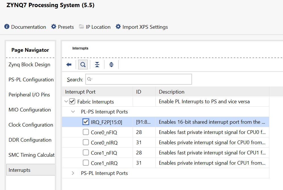
- IMPORTANT: is appears that after a “
Project Save as”, the top-levelsystem_wrapper.vhdis no more updated automatically when changes are made to in the Block design (a bug in 2020.2 version). This is an issue when the changes are related to external ports which is the case here! So, you need to remove thesystem_wrapper.vhdfrom the project (confirm deleting it from disk) and create a new wrapper by right-clicking onsystem.bd, and selectCreate HDL Wrapper…Leave theLet Vivado manage wrapper and auto-updateoption selected. - In the Flow Navigator, click
Run Synthesis. (ClickSaveif prompted).
C. Generate Bitstream and Export to Vitis⚓
- Generate the Bitstream.
- Export the hardware (
File > Export > Export Hardware), include the bitstream and choose a name for the Xilinx Shell Architecture (XSA) file, likehwtp2_wrapper. - Start Vitis by clicking
Tools > Launch Vitis IDE. IMPORTANT: note that when you copied the project fromHW_TP1through “save as”, only the hardware design has been copied. Therefore, you can create at this step a new workspace for Vitis related to HW_TP2 as follows: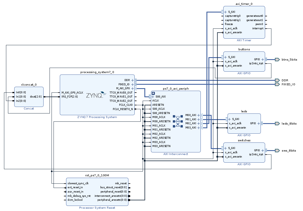
D. Software application development in Vitis⚓
- Create a new Application Project to test the embedded system peripherals. You have to follow the same steps as in the first lab (create a new platform based on the generated XSA file, give a name to the application project as
hwtp2_app, select anEmpty Applicationfor the template). - An application source code is provided in Moodle for this second lab, download it, and import it in the
srcfolder. - In a first step, test the UART, push-buttons, switches and LEDs without using the interrupts, e.g.:
- Display the status of the switches on the LEDs and on the UART terminal
- Increment/decrement a global variable through push-button commands and display its value on the UART. Use the software drivers (functions) provided by Xilinx to interface with the instantiated peripherals.
- Do the same tasks with activating the interrupts for the switches and the push-buttons. You need for that to uncomment the call to the function
SetupInterruptSystem()and to complete the missing code inside this function and in the corresponding interrupt handlers. - Add a functionality implementing the AXI Timer device and the management of its interrupt. For instance sending different values on the leds every second, different led display configurations controlled by the push-buttons, etc.
To be continued... !
Dernière mise à jour:
March 4, 2024